8-Bit GCD Digital System
A VHDL implementation of Euclid's subtraction algorithm using a datapath, Moore finite-state machine, simulation testbench, and physical Boolean Board verification.
Overview & Scope
This ELEG 29004 digital-design lab implements the greatest common divisor of two 8-bit unsigned values using the subtraction form of Euclid's algorithm. The hardware is divided into a datapath that stores and transforms the values and a Moore finite-state machine that generates the control sequence.
The course provided the top-level interface, datapath diagram, Double Dabble block, and simulation testbench. I integrated the datapath components and control logic in VHDL, implemented the FSM behavior, connected the display path, verified the design in simulation, and added the bonus zero-input error handling.
Top-Level Interface
The system accepts two 8-bit inputs, a start signal, clock, and active-high reset. Its output drives a four-digit seven-segment display.
| Signal | Width | Purpose |
|---|---|---|
| A | 8 bits | First unsigned input value |
| B | 8 bits | Second unsigned input value |
| start | 1 bit | Starts / restarts the calculation sequence |
| clk | 1 bit | Sequential clock |
| rst | 1 bit | Active-high reset |
| Dis | 7 bits | Seven-segment segment outputs |
| Disp_en | 4 bits | Display digit enables |
Datapath
The datapath stores A and B in 8-bit registers, compares the current values, and feeds them through conditional inversion and an 8-bit ripple-carry adder. Two multiplexers select whether each register loads the original input or the updated arithmetic result.
Subtraction is performed with two's-complement arithmetic: the selected operand is conditionally inverted and the ripple-carry adder performs the arithmetic. The comparator reports whether A equals B or A is greater than B, and those flags are used by the FSM to choose the next operation.
Moore Finite-State Machine
The control unit is a Moore machine, so the datapath-control outputs are determined by the current state. The machine repeatedly compares and subtracts until the two stored values are equal.
| State | Role | Main behavior |
|---|---|---|
| S0 | Idle | Waits for start. |
| S1 | Load | Loads the external A and B values into the registers. |
| S2 | Compare | Checks A = B and A > B to choose the next operation. |
| S3 | A > B | Computes A − B and stores the result back into A. |
| S4 | B > A | Computes B − A and stores the result back into B. |
| S5 | Display | Enables the result path once A and B are equal. |
| dS | Error | Handles a zero-valued input and prevents an infinite loop. |
Display Path
When the result state is reached, the value from register A is sent through a Double Dabble block to convert the 8-bit binary result into BCD data suitable for the multiplexed seven-segment display. The seven-segment decoder then determines which LED segments are active for each digit.
Zero-Input Error Handling
The subtraction-based algorithm assumes that both inputs are nonzero. If A or B is zero, repeatedly subtracting the smaller value would never converge. I added a dedicated dummy/error state that checks the inputs during the load phase and bypasses the normal calculation when a zero is detected.
I also modified the display path so this state produces a visible error indication: a leading zero followed by a simple sad-face pattern on the seven-segment display. The machine remains in the error state until the user starts a new operation.
Simulation Verification
Before programming the hardware, the design was tested with the provided simulation testbench. In addition to the external display outputs, I inspected the internal register value so the progression of Euclid's algorithm was easier to verify than by decoding the rapidly multiplexed seven-segment waveform.
| A | B | Expected result |
|---|---|---|
| 0 | 0 | Error state |
| 100 | 10 | 10 |
| 15 | 10 | 5 |
| 255 | 255 | 255 |
Boolean Board Hardware Test
After the simulation matched the expected state sequence, the generated bitstream was loaded onto a Boolean Board. The board switches provided the binary A and B values, and the calculated GCD was shown on the seven-segment display.
The board displayed 32, matching the expected result.
What I Learned
This project made the separation between datapath and control logic much more concrete. Rather than treating a digital system as one large block of logic, I had to think about where values are stored, which arithmetic operation is performed, how data is routed, and which state is responsible for asserting each control signal.
It also reinforced a useful verification workflow: simulate first, inspect internal signals when the top-level outputs are hard to interpret, and only then move to physical hardware.
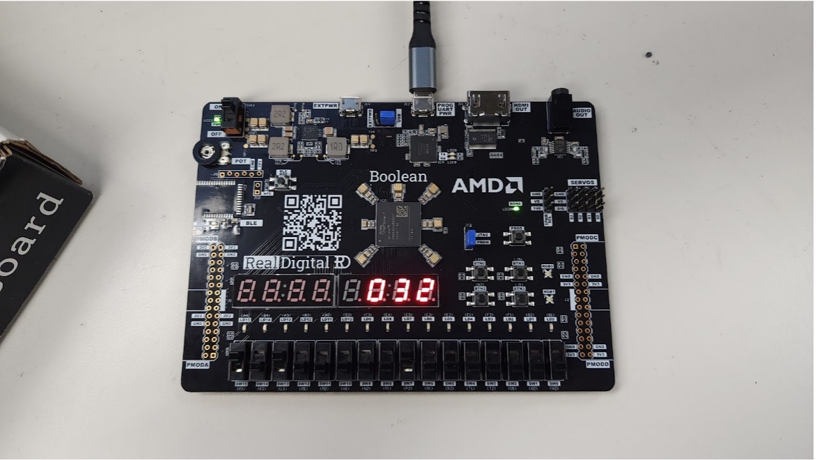
Final hardware test on the Boolean Board using input values A = 160 and B = 128. The VHDL implementation calculated and displayed the expected greatest common divisor of 32 on the seven-segment display.
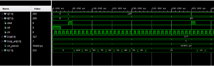
Simulation waveform used to verify the design before programming the FPGA. The trace shows the input values, clock, control signals, display outputs, and internal register value as the subtraction-based Euclidean algorithm progresses toward the final GCD.
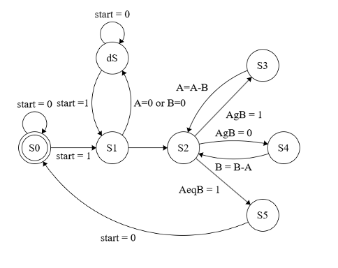
Control-state diagram for the GCD processor. The FSM handles input loading, comparison, A − B and B − A operations, result display, and the additional error state used when either input is zero.
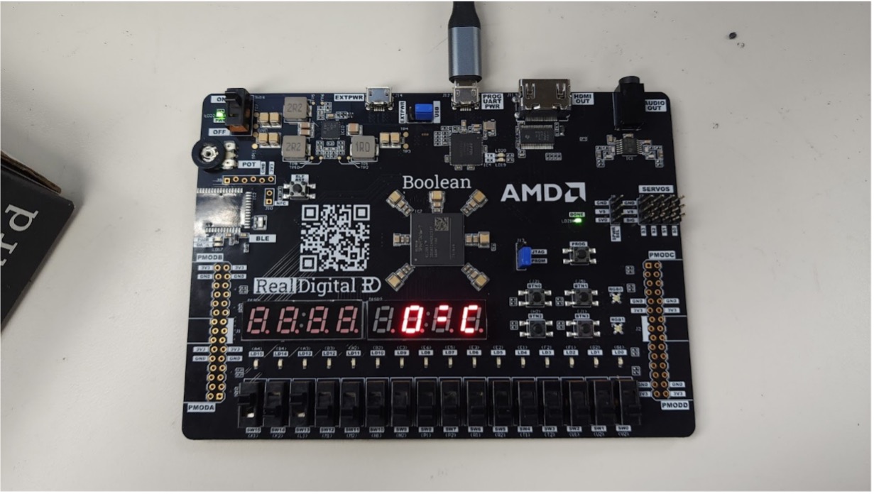
Hardware verification of the additional error state. When either input is zero, the controller avoids the infinite subtraction loop and displays a custom error indication on the seven-segment display.